
JP / EN


PRODUCTS
PRODUCTS
PRODUCTS
Laser system
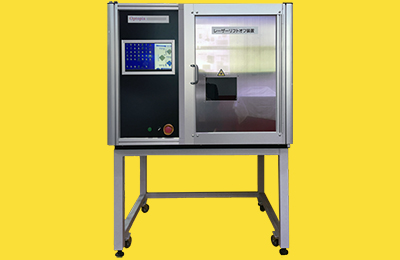
Laser Debonding Lab kit
Laser debonding (LDB) is a method of peeling the device formed the front side of the substrate by the laser from the back side.
This system is a compact system that can be used in electronic device laboratories and very easy operation.
Laser Debonding Lab kit
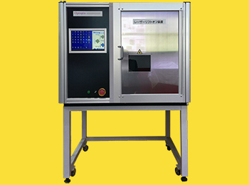
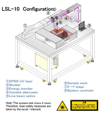
LDB Lab kit LSL-10
This system to form a uniform line beam using our original line beam optics and solid-state UV pulse laser .
It is an experimental device for performing the LLO process on the entire surface by moving the substrate on the stage while irradiating the substrate with the line beam. The software is already installed so that it can be easily controlled by a PC.
| LDB Lab kit LSL-10 specification | |
| Wavelength | 355nm |
| Line beam size | length 10mm × width 1mm |
| Energy density | 40 - 400mJ/cm2 Adjustable variable attenuator |
| Beam overlap | 0% - 98% use stage speed control |
| Work size | Max. 150mm × 150mm(option 370mm × 470mm) |
| Processing speed | 5mn / 100mm × 100mm |
| Stage stroke | 200mm × 200mm |
| System size | L1,200mm x W900mm x H1,300mm |
| Utility | AC100V ±10% 15A |
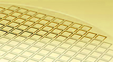
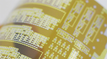
Laser Debonding application example
The laser debonding process (LDB) is used to peel off the device formed by the exposure process on the substrate from the backside of the substrate by laser in the flexible display process, LED manufacturing process, and thin film semiconductor process. As long as it is a material that can be laser ablated, a substrate that transmits laser light, such as glass or sapphire, can be used to rapidly peel off the interface because the interface can be instantaneously peeled off by laser irradiation. Laser debonding is also called laser lift-off.